Nanopatterning Market
- An Introduction to the Research Study
- Preface
- Market Taxonomy
- Definition of the Market and the Segments
- Acronyms and Assumptions
- The Research Procedure
- Sources of Data
- Secondary
- Primary
- Manufacturer Front
- End-User Front
- Calculation and Derivation of Market Size
- Top-Down Approach
- Bottom-up Approach
- Recommendation by Analyst for C-level Executives
- An Abstract of the Report
- Evaluation of Market Fluctuations and Outlook
- Market Growth Drivers
- Market Growth Deflation
- Market Trends
- Manufacturer Based
- End-User Based
- Fundamental Market Prospects
- Strategic Competitive Opportunities
- Geographic Opportunities
- Application Centric Opportunities
- Decarbonization Strategy and Carbon Credit Benefits for Market Players
- Global Government Decarbonization Plans/Goals by Each Country under 2015 Agreement Agreed by 200 Countries
- Measures taken by Countries to Reduce Carbon Footprints
- Carbon Credits and Subsidy Plans/Benefits Rolled out by the Government for Market Players
- Effective Ways to Harness Carbon-Credits and Impact on Profit Margins
- Demand Impact on the Companies Opting for Carbon Credits
- Regulatory & Standards Landscape
- Impact of Recession on Global and Japan Economy
- Economic Outlook: Japan
- Industry Risk Analysis
- Industry Value Chain Analysis
- Recent Trends/ Developments in Nanopatterning Market
- Patent Analysis
- Regional Analysis
- Product Type Analysis
- Application Analysis
- Product Feature Analysis
- PORTER Five Forces Analysis
- SWOT Analysis
- Global Nanopatterning Market Outlook
- Market Overview
- Market Value (USD Million) Current and Future Projections, 2020-2036
- Market Increment $ Opportunity Assessment, 2020-2036
- Year-on-Year (YoY) Growth Trend Analysis
- Global Nanopatterning Market Outlook & Projections, Opportunity Assessment by Segment, 2020-2036, By Type
- Nanoimprint Lithography Market Value USD Million) Current and Future Projections, 2020-2036
- E-beam Lithography Market Value (USD Million) Current and Future Projections, 2020-2036
- Photon-Based Nanolithography Market Value (USD Million) Current and Future Projections, 2020-2036
- Others Market Value (USD Million) Current and Future Projections, 2020-2036
- Global Nanopatterning Market Outlook & Projections, Opportunity Assessment by Segment, 2020-2036, By Application
- Healthcare Market Value (USD Million) Current and Future Projections, 2020-2036
- Organic Devices Market Value (USD Million) Current and Future Projections, 2020-2036
- Consumer Electronics Market Value (USD Million) Current and Future Projections, 2020-2036
- Others Market Value (USD Million) Current and Future Projections, 2020-2036
- Global Nanopatterning Market Segmentation Analysis (2020-2036), By Geography
- North America Market Value (USD Million) Current and Future Projections, 2020-2036
- Europe Market Value (USD Million) Current and Future Projections, 2020-2036
- Asia Pacific Excluding Japan Market Value (USD Million) Current and Future Projections, 2020-2036
- Japan Market Value (USD Million) Current and Future Projections, 2020-2036
- Latin America Market Value (USD Million) Current and Future Projections, 2020-2036
- Middle East & Africa Market Value (USD Million) Current and Future Projections, 2020-2036
- Global Nanopatterning Market Outlook & Projections, Opportunity Assessment by Segment, 2020-2036, By Type
- Cross Analysis of Type w.r.t. Application (USD Million), 2023-2036
- North America Nanopatterning Market Outlook
- Outline of the Segment
- Detailed Overview
- Market Value (USD Million) Current and Future Projections, 2020-2036
- Recent trends in the market
- Market Players
- North America Nanopatterning Market Outlook & Projections, Opportunity Assessment by Segment, 2020-2036, By Type
- Nanoimprint Lithography Market Value USD Million) Current and Future Projections, 2020-2036
- E-beam Lithography Market Value (USD Million) Current and Future Projections, 2020-2036
- Photon-Based Nanolithography Market Value (USD Million) Current and Future Projections, 2020-2036
- Others Market Value (USD Million) Current and Future Projections, 2020-2036
- North America Nanopatterning Market Outlook & Projections, Opportunity Assessment by Segment, 2020-2036, By Application
- Healthcare Market Value (USD Million) Current and Future Projections, 2020-2036
- Organic Devices Market Value (USD Million) Current and Future
- Consumers Electronics Market Value (USD Million) Current and Future Projections, 2020-2036
- Others Market Value (USD Million) Current and Future Projections, 2020-2036
- North America Nanopatterning Market Segmentation Analysis (2020-2036), By Country
- US Market Value (USD Million) Current and Future Projections, 2020-2036
- Canada Market Value (USD Million) Current and Future Projections, 2020-2036
- North America Nanopatterning Market Outlook & Projections, Opportunity Assessment by Segment, 2020-2036, By Type
- Cross Analysis of Type w.r.t. Application (USD Million), 2023-2036
- Europe Nanopatterning Market Outlook
- Outline of the Segment
- Detailed Overview
- Market Value (USD Million) Current and Future Projections, 2020-2036
- Recent trends in the market
- Market Players
- Europe Nanopatterning Market Outlook & Projections, Opportunity Assessment by Segment, 2020-2036, By Type
- Europe Nanopatterning Market Outlook & Projections, Opportunity Assessment by Segment, 2020-2036, By Application
- Europe Nanopatterning Market Segmentation Analysis (2020-2036), By Country
- UK Market Value (USD Million) Current and Future Projections, 2020-2036
- Germany Market Value (USD Million) Current and Future Projections, 2020-2036
- France Market Value (USD Million) Current and Future Projections, 2020-2036
- Italy Market Value (USD Million) Current and Future Projections, 2020-2036
- Spain Market Value (USD Million) Current and Future Projections, 2020-2036
- BENELUX Market Value (USD Million) Current and Future Projections, 2020-2036
- Poland Market Value (USD Million) Current and Future Projections, 2020-2036
- Russia Market Value (USD Million) Current and Future Projections, 2020-2036
- Rest of Europe Market Value (USD Million) Current and Future Projections, 2020-2036
- Cross Analysis of Type w.r.t. Application (USD Million), 2023-2036
- Asia Pacific Nanopatterning Market Outlook
- Outline of the Segment
- Detailed Overview
- Market Value (USD Million) Current and Future Projections, 2020-2036
- Recent trends in the market
- Market Players
- Asia Pacific Excluding Japan (APEJ) Nanopatterning Market Outlook & Projections, Opportunity Assessment by Segment, 2020-2036, By Type
- Asia Pacific Excluding Japan (APEJ) Nanopatterning Market Outlook & Projections, Opportunity Assessment by Segment, 2020-2036, By Application
- Asia Pacific Excluding Japan (APEJ) Nanopatterning Market Outlook & Projections, Opportunity Assessment by Segment, 2020-2036, By Country
- China Market Value (USD Million) Current and Future Projections, 2020- 2036 • Malaysia Market Value (USD Million) Current and Future Projections, 2020- 2036
- India Market Value (USD Million) Current and Future Projections, 2020-2036
- Indonesia Market Value (USD Million) Current and Future Projections, 2020- 2036
- South Korea Market Value (USD Million) Current and Future Projections, 2020-2036
- Thailand Market Value (USD Million) Current and Future Projections, 2020- 2036 • Vietnam Market Value (USD Million) Current and Future Projections, 2020- 2036 • Australia Market Value (USD Million) Current and Future Projections, 2020- 2036
- Rest of Asia Pacific Excluding Japan (APEJ) Market Value (USD Million) Current and Future Projections, 2020-2036Nanoimprint Lithography Market Value USD Million) Current and Future Projections, 2020-2036
- Cross Analysis of Type w.r.t. Application (USD Million), 2023-2036
- Japan Nanopatterning Market Outlook
- Outline of the Segment
- Detailed Overview
- Market Value (USD Million) Current and Future Projections, 2020-2036
- Recent trends in the market
- Market Players
- Japan Nanopatterning Market Outlook & Projections, Opportunity Assessment by Segment, 2020-2036, By Type
- Japan Nanopatterning Market Outlook & Projections, Opportunity Assessment by Segment, 2020-2036, By Application
- Cross Analysis of Type w.r.t. Application (USD Million)
- Latin America Nanopatterning Market Outlook
- Outline of the Segment
- Detailed Overview
- Market Value (USD Million) Current and Future Projections, 2020-2036
- Recent trends in the market, 2023-2036
- Market Players
- Latin America Nanopatterning Market Outlook & Projections, Opportunity Assessment by Segment, 2020-2036, By Type
- Latin America Nanopatterning Market Outlook & Projections, Opportunity Assessment by Segment, 2020-2036, By Application
- Latin America Nanopatterning Market Segmentation Analysis (2020-2036), By Country
- Mexico Market Value (USD Million) Current and Future Projections, 2020-2036
- Argentina Market Value (USD Million) Current and Future Projections, 2020-2036
- Brazil Market Value (USD Million) Current and Future Projections, 2020-2036
- Rest of Latin America Market Value (USD Million) Current and Future Projections, 2020-2036
- Cross Analysis of Type w.r.t. Application (USD Million), 2023-2036
- Middle East & Africa Nanopatterning Market Outlook
- Outline of the Segment
- Detailed Overview
- Market Value (USD Million) Current and Future Projections, 2020-2036
- Recent trends in the market
- Market Players
- Middle East & Africa Nanopatterning Market Outlook & Projections, Opportunity Assessment by Segment, 2020-2036, By Type
- Middle East & Africa Nanopatterning Market Outlook & Projections, Opportunity Assessment by Segment, 2020-2036, By Application
- Middle East & Africa Nanopatterning Market Segmentation Analysis (2020-2036) By Country
- GCC Market Value (USD Million) Current and Future Projections, 2020-2036
- Israel Market Value (USD Million) Current and Future Projections, 2020-2036
- South Africa Market Value (USD Million) Current and Future Projections, 2020-2036
- Rest of Middle East & Africa Market Value (USD Million) Current and Future Projections, 2020-2036
- Cross Analysis of Type w.r.t. Application (USD Million), 2023-2036
- Competitive Model: A Detailed Inside View for Investors
- Company Market Share (2022)
- Business Profile of Key Enterprise
- AMO GmbH
- EV Group (EVG)
- SVG Optronics, Co., Ltd.
- IMS CHIPS
- NIL TECHNOLOGY
- Vistec Electron Beam GmbH
- Nanoscribe GmbH & Co. KG
- Obducat AB
- Micro Resist Technology Gmbh
- SET Corporation SA
- Raith GmbH
- Major Japanese Players
- TOPPAN Inc.
- NTT Advanced Technology Corporation
- Canon Inc.
- KYODO INTERNATIONAL, INC.
Nanopatterning Market Outlook:
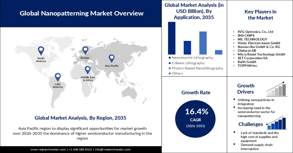
Nanopatterning Market size was over USD 3.29 billion in 2025 and is projected to reach USD 15.02 billion by 2035, growing at around 16.4% CAGR during the forecast period i.e., between 2026-2035. In the year 2026, the industry size of nanopatterning is evaluated at USD 3.78 billion.

The market for nanopatterning is anticipated to grow in the upcoming years due to the development of healthcare infrastructure. The WHO data indicates that the fastest growth in global health spending is concentrated in low- and middle-income countries, where average annual growth rates are 6%, while high-income countries have average growth rates of 4%. Furthermore, approximately 35% of health spending in a nation comes from out-of-pocket expenses, with governments typically footing the bill for 51% of the total.
In addition to these, the market for nanopatterning is expanding globally due to the increasing need for smaller electronic gadgets, which is also drastically altering the high-tech and semiconductor production industries. This need is being driven by consumer desires for items that are more functional, stylish, and portable. Nanopatterning is crucial because it allows precise patterns and structures to be made at the nanoscale, which is necessary to meet the stringent standards of miniaturization.
Key Nanopatterning Market Insights Summary:
Regional Highlights:
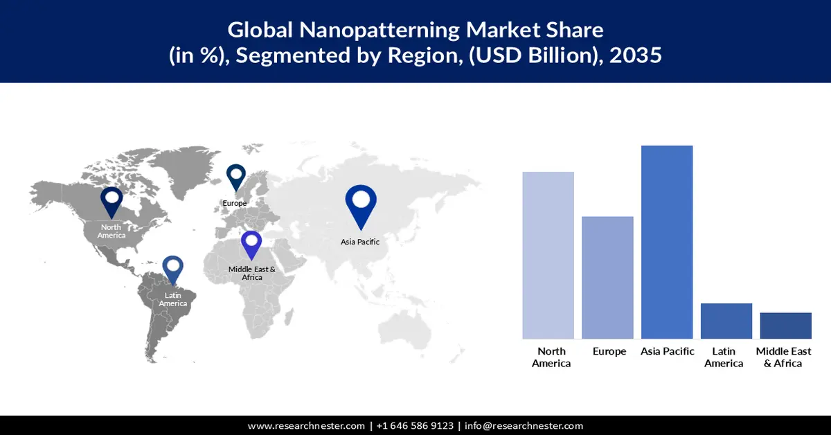
- Asia Pacific nanopatterning market is anticipated to secure a lucrative share, driven by the region’s dominance in semiconductor manufacturing and technological innovation.
- By 2035, North America is expected to hold a considerable share, supported by rising demand for advanced electronic devices and semiconductors for consumer applications.
Segment Insights:
- By 2035, the nanoimprint lithography segment is projected to hold a remarkable share, propelled by its capability to create highly precise nanoscale patterns for semiconductor and photonics applications.
- The consumer electronics segment is expected to capture a notable share by 2035, driven by demand for smaller, more efficient devices with enhanced functionality and lower energy consumption.
Key Growth Trends:
- Developments in Nanomaterials and the Expanding Field of Nanopatterning Applications
- Increasing Need in the Semiconductor Sector for Nanopatterning
Major Challenges:
- Lack of standards and the high cost of supplies and equipment
- Lack of skilled personnel may impede growth of the market.
Key Players: EV Group (EVG), SVG Optronics, Co., Ltd, IMS CHIPS, NIL TECHNOLOGY, Vistec Electron beam GmbH, Nanoscribe GmbH & Co. KG, Obducat AB, Micro Resist Technology GmbH, SET Corporation SA, Raith GmbH, TOPPAN Inc., NTT Advanced Technology Corporation, Canon Inc., Kyodo International Inc.
Global Nanopatterning Market Forecast and Regional Outlook:
Market Size & Growth Projections:
- 2025 Market Size: USD 3.29 billion
- 2026 Market Size: USD 3.78 billion
- Projected Market Size: USD 15.02 billion by 2035
- Growth Forecasts: 16.4%
Key Regional Dynamics:
- Largest Region: Asia Pacific
- Fastest Growing Region: North America
- Dominating Countries: China, United States, Taiwan, South Korea, Japan
- Emerging Countries:India, Singapore, Malaysia, Brazil, Germany
Last updated on : 26 November, 2025
Nanopatterning Market - Growth Drivers and Challenges
Growth Drivers
-
Developments in Nanomaterials and the Expanding Field of Nanopatterning Applications- In recent years, significant advancements have been made in nanopatterning and nanoimprint lithography. There is an overwhelming need to customize the surface at the micro and nanoscale. It makes handling and operating at the Nano and microscale levels easier. Its uses in the medical industry are expanding daily. The global nanopatterning market is expanding due in large part to the development of nanomaterials. In order to incorporate these nanomaterials into device structures, nanopatterning is essential. Recently, there has been a lot of interest in science due to the possible uses of Lithography-based nanopatterning in biosensors, solar cells, anti-reflection and anti-fingerprint films, nanofluidic and microfluidic channels, and some functional optical films.
-
Increasing Need in the Semiconductor Sector for Nanopatterning- The desire for smaller, quicker, and more powerful electronic devices combined with the rapid improvements in semiconductor technology should propel the worldwide nanopatterning industry's growth. The semiconductor industry's increasing need for nanopatterning is anticipated to last as device makers work to make devices that are more compact, potent, and effective. The fabrication process will see a growing reliance on nanopatterning, which will allow for the development of next-generation technologies that will improve our daily lives and transform a number of industries. The need for nanopatterning is also being driven by the growing use of nanomaterials in semiconductors, in addition to these other considerations. Due to a shift in the location of electronic equipment production, the Asia Pacific market outperformed all other regional markets in terms of sales in 2001, according to the Semiconductor Industry Association. Since then, its size has increased dramatically, rising from USD 39.8 billion to over USD 271 billion in 2020. China accounted for 56% of the Asia Pacific market and 34% of the global market, making it by far the largest country market in the Asia Pacific area.
-
Utilizing Nanoparticles in Integration- The emphasis on integrating nanopatterning techniques with nanomaterials to create synergies that enhance their respective capabilities. Because of the special qualities of nanomaterials and their potential to improve the functionality and performance of nanopatterned devices, the integration of nanomaterials into nanopatterning is a trend that is rapidly expanding in the worldwide nanopatterning market. The ongoing discovery of novel nanomaterials with enhanced capabilities and the growing need for high-performance, multifunctional devices across multiple industries are expected to fuel the trend of using nanomaterials into nanopatterning. Through this combination, novel nanopatterned devices with enhanced functionality, performance, and sustainability will be formed, revolutionizing a number of industries and improving our daily lives.
Challenges
-
Lack of standards and the high cost of supplies and equipment- Operating nanopatterning equipment necessitates specialized knowledge due to its intricate nature. Due to the increased cost of the equipment, small and medium-sized businesses (SMEs) find it challenging to enter the market. Furthermore, the materials required for nanopatterning are sometimes pricy and challenging to find. Also, the industry lacks standardization and nanopatterning is a relatively new technology. This may result in compatibility problems and make it challenging for vendors to cooperate. Furthermore, the absence of standardization may result in increased expenses and make it challenging for clients to compare various nanopatterning solutions.
-
Lack of skilled personnel may impede growth of the nanopatterning market.
-
Demand supply chain disruption may hinder the growth of the market.
Nanopatterning Market Size and Forecast:
| Report Attribute | Details |
|---|---|
|
Base Year |
2025 |
|
Forecast Year |
2026-2035 |
|
CAGR |
16.4% |
|
Base Year Market Size (2025) |
USD 3.29 billion |
|
Forecast Year Market Size (2035) |
USD 15.02 billion |
|
Regional Scope |
|
Nanopatterning Market Segmentation:
Type Segment Analysis
Nanoimprint lithography segment is expected to hold remarkable nanopatterning market share by 2035. The segment's expansion can be attributed to its capacity to produce very precise and resolute nanoscale designs. In order to replicate complex patterns onto a substrate, nanoimprint lithography uses a template to mechanically distort a resist material. The use of nanoimprint lithography has grown across a number of industries, most notably semiconductor manufacturing, where the technology's high-resolution capabilities enable the production of smaller, more effective devices. Global semiconductor sales increased by more than 30% in just two years, to reach 618 billion dollars in 2022. Moreover, EV Group (EVG) and Toppan Photomask Co. Ltd. announced in September 2022 that they would be working together to promote nanoimprint lithography (NIL) as a high-volume manufacturing (HVM) method for the photonics sector.
Application Segment Analysis
In nanopatterning market, consumer electronics segment is set to capture noteworthy revenue share by the end of 2035. The market for nanopatterning in consumer electronics is propelled by the need for reduced size, enhanced functionality, and reduced energy consumption. The development of sensors for better functionality, display technology for better screens, and semiconductor fabrication for smaller, more powerful chips are important fields. For example, ASML is essential to the fabrication of semiconductor photolithography equipment.
Our in-depth analysis of the global nanopatterning market includes the following segments:
|
Type |
|
|
Application |
|

Vishnu Nair
Head - Global Business DevelopmentCustomize this report to your requirements — connect with our consultant for personalized insights and options.
Nanopatterning Market - Regional Analysis
APAC Market Insights
In nanopatterning market, Asia Pacific region is anticipated to capture lucrative revenue share by the end of 2035. The main factor driving the APAC nanopatterning market is the dominance of semiconductor manufacturing, which is fueled by the strong demand for electronics products and technical innovation. Taiwan, China, and South Korea are well-known as major global centres for the production of semiconductors. The expansion of the nanopatterning market in the area is closely related to the growth of the semiconductor sector. By itself, Taiwan Semiconductor Manufacturing Co. (TSMC) holds half of the market. produces chips for Qualcomm, AMD, Nvidia, and Apple. Furthermore, China is expected to account for 25% of global semiconductor sales by 2030, up from 9% currently. Furthermore, a dynamic ecosystem encompassing semiconductor production, design, and innovation is collectively formed by nations like China, South Korea, Singapore, and Malaysia. The demand for nanopatterning in the APAC area is strong due to its prominence in the semiconductor sector.
North American Market Insights
North America region is projected to hold considerable nanopatterning market share by 2035. One of the main factors propelling the North American nanopatterning market is the rising need for sophisticated electronic devices. The demand for semiconductors is rising in tandem with the need for consumer applications like smartphones. In 2021, mobile advertising reached a global value of USD 288 billion.

Nanopatterning Market Players:
- AMO GmbH
- Company Overview
- Business Strategy
- Key Product Offerings
- Financial Performance
- Key Performance Indicators
- Risk Analysis
- Recent Development
- Regional Presence
- SWOT Analysis
- EV Group (EVG)
- SVG Optronics, Co., Ltd
- IMS CHIPS
- NIL TECHNOLOGY
- Vistec Electron beam GmbH
- Nanoscribe GmbH & Co. KG
- Obducat AB
- Micro Resist Technology GmbH
- SET Corporation SA
- Raith GmbH
- TOPPAN Inc.
- NTT Advanced Technology Corporation
- Canon Inc.
- Kyodo International Inc.
Recent Developments
- NIL Technology ApS, one of the leaders in nanoimprint lithography, announced the closure of USD 7.4 million of funding jointly funded by NGP Capital and Jolt Capital. NIL Technology ApS will use this fund to globally expand its research and development activities, distribution footprint, and manufacturing capacity.
- Micro resist technology GmbH announced the joint venture with SÜSS MicroTec SE. This partnership will enable Micro resist technology GmbH to expand its production capacity and nanoimprint lithography deployment
- Report ID: 5454
- Published Date: Nov 26, 2025
- Report Format: PDF, PPT
- Explore a preview of key market trends and insights
- Review sample data tables and segment breakdowns
- Experience the quality of our visual data representations
- Evaluate our report structure and research methodology
- Get a glimpse of competitive landscape analysis
- Understand how regional forecasts are presented
- Assess the depth of company profiling and benchmarking
- Preview how actionable insights can support your strategy
Explore real data and analysis
Frequently Asked Questions (FAQ)
Nanopatterning Market Report Scope
Free Sample includes current and historical market size, growth trends, regional charts & tables, company profiles, segment-wise forecasts, and more.
Connect with our Expert
Copyright @ 2026 Research Nester. All Rights Reserved.


