Semiconductor Inspection System Market Outlook:
Semiconductor Inspection System Market size was over USD 7.24 billion in 2025 and is poised to exceed USD 15.78 billion by 2035, witnessing over 8.1% CAGR during the forecast period i.e., between 2026-2035. In the year 2026, the industry size of semiconductor inspection system is estimated at USD 7.77 billion.
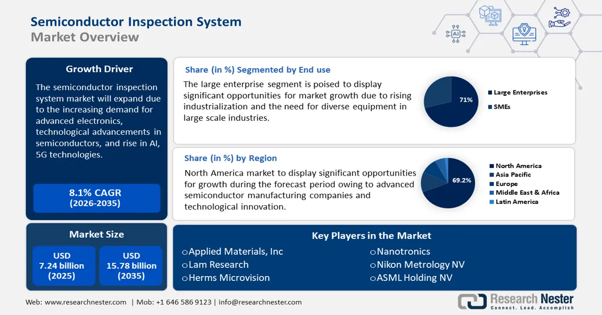
The primary growth driver of the semiconductor inspection system market is the increasing demand for advanced electronics such as smartphones, daily wearables, laptops, televisions, and IoT devices. This is driving the need for semiconductors, which in turn can increase the demand for inspection systems. The semiconductor inspection system market is experiencing significant growth driven by the expansion of the semiconductor industry. In 2023, nearly 1 trillion semiconductors were sold globally. The Semiconductor Industry Association (SIA) revealed that global semiconductor sales recorded USD 57.8 billion in November 2024. The sales increased by 20.7% compared to November 2023 sales of USD 47.9 billion.
Growing investments in semiconductor fabrication facilities and increased production capacity globally fuel the need for inspection systems. The trend towards smaller transistors and more intricate designs increases the risk of defects, driving the demand for advanced inspection solutions. Semiconductors and IoT have already occupied the Wearable technology industry, smart-home appliances, medical electronics, Industrial automation, Autonomous vehicles, and help in traffic control.
Key Semiconductor Inspection System Market Insights Summary:
Regional Highlights:
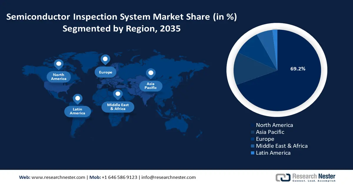
- North America dominates the Semiconductor Inspection System Market with a 69.2% share, fueled by advanced semiconductor manufacturing and technological innovation, positioning it as a global leader through 2026–2035.
- Asia Pacific's semiconductor inspection system market is expected to grow the fastest by 2035, fueled by rising demand for low-cost semiconductors and industrial expansion in China, Japan, South Korea, and India.
Segment Insights:
- The Wafer segment is anticipated to see rapid revenue growth by 2035, driven by the expansion of the semiconductor industry and rising demand for high-performance chips.
- The Large Enterprise segment of the Semiconductor Inspection System Market is projected to hold a 71% share by 2035, fueled by rising industrialization and the need for efficient large-scale assembly solutions.
Key Growth Trends:
- Technological advancements in semiconductors
- Shift towards AI, 5G, and autonomous technologies
Major Challenges:
- High cost of equipment
- Complexity of semiconductor designs
- Key Players: Applied Materials, Inc, Herms Microvision, Lam Research, Nanotronics, Rudolph Technologies, Inc., Nanometrics, Inc., KLA-Tencor Corporation, Nikon Metrology NV.
Global Semiconductor Inspection System Market Forecast and Regional Outlook:
Market Size & Growth Projections:
- 2025 Market Size: USD 7.24 billion
- 2026 Market Size: USD 7.77 billion
- Projected Market Size: USD 15.78 billion by 2035
- Growth Forecasts: 8.1% CAGR (2026-2035)
Key Regional Dynamics:
- Largest Region: North America (69.2% Share by 2035)
- Fastest Growing Region: Asia-Pacific
- Dominating Countries: United States, Japan, South Korea, Germany, Canada
- Emerging Countries: China, India, Japan, South Korea, Taiwan
Last updated on : 13 August, 2025
Semiconductor Inspection System Market Growth Drivers and Challenges:
Growth Drivers
- Technological advancements in semiconductors: Innovations such as smaller node sizes, 3D packaging, and complex architectures in semiconductor manufacturing require high-precision inspection systems, particularly e-beam and optical technologies. Technological advancements in semiconductors have led to an increase in demand for electronic products thus increasing the sale of electronic goods. For instance, according to the U.S. International Trade Commission, the total export of electronic products in the U.S. remarkably increased by 12.9% from USD 32.5 billion in 2020 to USD 285.8 billion in 2021. In addition, top manufacturing firms are competing to develop miniature semiconductor chips. For instance, in March 2024, Marvell Technology Inc. collaborated with TSMC to become the industry’s first technology platform to develop 2nm semiconductors optimized for accelerated infrastructure. This is also expected to boost the global semiconductor inspection system market growth during the forecast period.
- Shift towards AI, 5G, and autonomous technologies: Applications in AI, 5G networks, and autonomous vehicles demand highly sophisticated and reliable semiconductors that require strict inspection standards. Further, automation, real-time monitoring, and AI-driven analytics in semiconductor manufacturing create demand for inspection systems that can integrate with these technologies for enhanced defect detection. According to a 2023 report published by IEEE International Roadmap for Devices and Systems, using AI and IoT has brought innovation to the semiconductor industry. The integration of IoT can turn ordinary objects into smart devices and create better economic opportunities.
Challenges
- High cost of equipment: Advanced semiconductor inspection systems particularly e-beam and multi-beam systems are expensive. The high upfront investment limits adoption, especially for small and medium-sized enterprises. Moreover, rapid technological advancements and fast evolution require continuous updates and development in inspection systems making it challenging for manufacturers to keep pace with industry needs. With the development of new technology nodes, the design costs are increasing.
- Complexity of semiconductor designs: The increasing complexity of semiconductors, chips such as 3D stacking, smaller node sizes, and FinFET architectures makes detection more challenging and thus demands constant innovation in inspection systems. Additionally, the shortage of skilled trained professionals, technicians, and engineers also poses a threat to the semiconductor inspection system market. According to the Semiconductor Industry Association (SIA), the U.S. semiconductor design industry is predicted to face a shortage of 23,000 design workers by 2030. Thus, operating and maintaining advanced inspection systems requires a skilled workforce.
Semiconductor Inspection System Market Size and Forecast:
| Report Attribute | Details |
|---|---|
|
Base Year |
2025 |
|
Forecast Period |
2026-2035 |
|
CAGR |
8.1% |
|
Base Year Market Size (2025) |
USD 7.24 billion |
|
Forecast Year Market Size (2035) |
USD 15.78 billion |
|
Regional Scope |
|
Semiconductor Inspection System Market Segmentation:
Type (Wafer and Mask)
The wafer segment in semiconductor inspection system market is estimated to register rapid revenue growth during the forecast period owing to rapid expansion of the semiconductor industry, rising advancements in consumer electronics, and growing demand for high-performance and low-cost semiconductors. As industries such as AI, automotive, and 5G require chips with superior reliability, it increases the need for thorough wafer inspections to meet strict quality standards. Top companies are constantly working towards research and development for efficient semiconductors. For instance, in July 2023 Applied Materials, Inc. introduced Vistara which is the most significant and innovative wafer manufacturing platform in over a decade. This platform is designed to provide chipmakers with the flexibility, intelligence, and sustainability needed to tackle growing chipmaking challenges.
End use (SMEs and Large enterprises)
Large enterprise segment is anticipated to dominate around 71% semiconductor inspection system market share by the end of 2035, owing to rising industrialization and the need for diverse equipment in large-scale assembly. Large enterprises are increasingly investing in semiconductor inspection systems to enhance production efficiency, ensure product quality, and meet the growing demands for advanced technological applications. Moreover, the growing need for faster, compact, low-power, and high-performance devices to cater to the complexity of large-scale assemblies has resulted in the rising adoption of sophisticated inspection systems in these organizations.
Our in-depth analysis of the global market includes the following segments:
|
Type |
|
|
End use |
|

Vishnu Nair
Head - Global Business DevelopmentCustomize this report to your requirements — connect with our consultant for personalized insights and options.
Semiconductor Inspection System Market Regional Analysis:
North America Market Forecast
North America in semiconductor inspection system market is anticipated to hold more than 69.2% revenue share by 2035, driven by advanced semiconductor manufacturing and the region’s focus on technological innovation. The presence of leading companies such as Applied Materials, Intel, and Texas Instruments supports demand for inspection systems. Further, government initiatives to boost domestic chip production such as CHIPS Act, are fuelling market growth. Additionally, strong R&D capabilities in North America contribute to the development and adoption of new inspection technologies.
The U.S. semiconductor inspection system market is driven by strong domestic production and continuous investments in advanced chip manufacturing technologies. The SIA reported that the U.S. semiconductor industry accounts for half of the overall market and has displayed steady annual growth in 2023. Moreover, initiatives like the CHIPS and Science Act aim to enhance semiconductor production and boost the demand for inspection systems. The U.S. also excels in R&D encouraging innovation in inspection technologies to meet the needs of emerging nodes and applications.
The semiconductor inspection system market in Canada is experiencing steady growth, supported by various factors including the growing semiconductor manufacturing and design ecosystem. The country supports the industry through government incentives and collaborations with global semiconductor players. Canada majorly focuses on innovation and investing in developing specialized applications for steady growth. For instance, in April 2024, the Prime Minister announced USD 1.75 billion for AI-related investments, and about USD 1.5 billion for a new AI Compute Access Fund aimed at providing access to computing capabilities and technical infrastructure. The government also allocated USD 36.5 million to develop an AI safety institute to address risks from harmful AI systems. Additionally, USD 136.7 million was invested to expand chip packaging and R&D at IBM Canada’s Bromont plant.
Asia Pacific Market Analysis
The semiconductor inspection system market of Asia Pacific is poised to achieve the fastest growth by 2035. The growth can be attributed to rising demand for high-performance, low-cost semiconductors and the expansion of the semiconductor industry in China, Japan, South Korea, and India. In addition to this, the growing demand for advanced semiconductors in industries such as electronics, automotive, and telecommunications is expected to increase the adoption of semiconductor inspection systems in the coming years.
The semiconductor inspection system market in China is rapidly expanding as it is a major hub for semiconductor manufacturing and consumption. With increasing investments in domestic semiconductor production, the country is focusing on improving the quality and efficiency of its manufacturing processes through advanced inspection systems. The adoption of AI-driven and automated inspection technologies is enhancing defect detection and process control. According to a report by the Information Technology and Innovation Foundation released in August 2024, the number of semiconductor design firms in China has increased nearly sixfold, from 582 to 3,243 from 2010 to 2022.
The semiconductor inspection system market in India is experiencing steady growth attributed to the country’s rising demand for electronics and technological advancements in semiconductor manufacturing. As India strengthens its domestic semiconductor production capabilities, the need for high-precision inspection systems is increasing to ensure quality and reliability. Furthermore, the adoption of AI and automation in inspection processes is helping Indian manufacturers enhance efficiency and reduce defects. In 2022, India’s central government launched the Semicon India Programme worth USD 10 billion, coupled with incentives from Indian states for manufacturing and design. Further, the Indian Semiconductor Mission (ISM), recently approved proposals for facilitating growth of three semiconductor plants.
Key Semiconductor Inspection System Market Players:
- Applied Materials, Inc.
- Company Overview
- Business Strategy
- Key Product Offerings
- Financial Performance
- Key Performance Indicators
- Risk Analysis
- Recent Development
- Regional Presence
- SWOT Analysis
- Herms Microvision
- Lam Research
- Nanotronics
- Rudolph Technologies, Inc.
- Nanometrics, Inc.
- KLA-Tencor Corporation
- Nikon Metrology NV
- Thermo Fisher Scientific, Inc.
- ASML Holding NV
The semiconductor inspection system market is led by key players alongside several specialized companies, all striving to innovate and meet the evolving demands of semiconductor manufacturing. KLA Corporation, Applied Materials, Inc., Onto Innovation, ViSCO Technologies, TAKANO Co. Ltd, and JAI are some key players contributing to the market. Here is a list of key players operating in the global semiconductor inspection system market:
Recent Developments
- In January 2024, Cohu, a global supplier of equipment and services announced the launch of AI inspection software that provides real time computation for semiconductor manufacturers to improve visual inspection accuracy at production speeds.
- In April 2022, ASML Holdings N.V. launched HMI eScan 1100, the first multiple e-beam wafer inspection system for in-line yield enhancement applications, including voltage contrast defect inspection and physical defect inspection.
- Report ID: 7085
- Published Date: Aug 13, 2025
- Report Format: PDF, PPT
- Explore a preview of key market trends and insights
- Review sample data tables and segment breakdowns
- Experience the quality of our visual data representations
- Evaluate our report structure and research methodology
- Get a glimpse of competitive landscape analysis
- Understand how regional forecasts are presented
- Assess the depth of company profiling and benchmarking
- Preview how actionable insights can support your strategy
Explore real data and analysis
Frequently Asked Questions (FAQ)
Free Sample includes current and historical market size, growth trends, regional charts & tables, company profiles, segment-wise forecasts, and more.
Connect with our Expert


Copyright @ 2026 Research Nester. All Rights Reserved.
