Semiconductor Inspection Microscope Market Outlook:
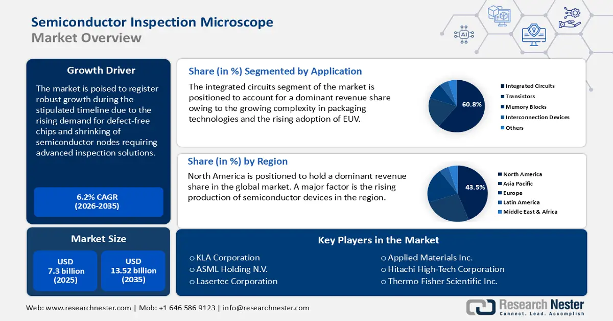
Semiconductor Inspection Microscope Market size was over USD 7.3 billion in 2025 and is poised to exceed USD 13.32 billion by 2035, growing at over 6.2% CAGR during the forecast period i.e., between 2026-2035. In the year 2026, the industry size of semiconductor inspection microscope is estimated at USD 7.71 billion.
The semiconductor inspection microscope market is exhibiting rapid growth attributed to the rising demand for defect-free chips. With the trends highlighting semiconductor nodes shrinking to 3nm and beyond, the demand for high-resolution optical, electron, and laser-based inspection systems to detect sub-micron defects. Moreover, the push for high bandwidth memory (BHM) is accelerating the adoption of next-gen microscopy solutions that offer automated, real-time defect detection and metrology-grade precision. The table below highlights the global semiconductor sales figures which align with the rising demand for semiconductor inspection microscope.
Global Semiconductor Sales Figures
|
Particulars |
Details (2022) |
|
Global semiconductor sales in a decade (2012 to 2022) |
USD 602 billion |
|
Share of logic chips in the global semiconductor sales |
42% |
|
Memory chips share in semiconductor sales |
28% |
|
Analog share in semiconductor sales |
13% |
|
Optoelectronics share in semiconductor sales |
8% |
|
Sensors share in semiconductor sales |
6% |
|
Largest semiconductor application |
Communications with 30% share |
Source: Congressional Research Service (CRS)
Furthermore, trends highlight that semiconductor manufacturers are moving towards 3D packaging while companies are investing in wafer-level inspection tools to ensure quality standards are maintained. The trends are beneficial for the growth of the semiconductor inspection microscope with inspection microscopes being positioned as vital in ensuring structural integrity. In November 2024, CHIPS for America announced funding worth USD 300 million in advanced packaging research projects in California, Arizona, and Georgia to accelerate the development of cutting-edge technologies for the semiconductor sector. The investment is predicted to drive demand for high-precision inspection microscopes for nanometer-level of defect detection.
Two major factors which are influencing the industry’s growth are the Industry 4.0 initiatives and fab automations, accelerating the requirement for smart, connected inspection solutions enabling predictive maintenance. The market analysis predicts that startups and niche players that specialize in non-destructive, high-speed inspection methods will attract significant investment. For instance, in July 2024, Nearfield Instruments announced securing of USD 140.0 million worth of funding in the Series C round. Additionally, with semiconductor nodes becoming more intricate, the demand for next-generation microscopes is expected to experience continues growth assisting a steady semiconductor inspection microscope market growth by the end of 2035.
Key Semiconductor Inspection Microscope Market Insights Summary:
Regional Insights:
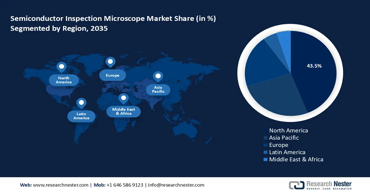
- North America semiconductor inspection microscope market is projected to hold over 43.5% share by 2035 as its robust semiconductor manufacturing ecosystem fuels consistent demand for advanced inspection tools stemming from its well-established semiconductor manufacturing ecosystem.
- APAC semiconductor inspection microscope market is anticipated to grow rapidly through 2026–2035 supported by the substantial semiconductor manufacturing base across China, Japan, South Korea, Taiwan, and India.
Segment Insights:
- Integrated circuits (IC) segment is expected to capture over 60.8% share by 2035 in the semiconductor inspection microscope market as its dominance strengthens owing to the rising complexity of packaging technologies.
- Electron microscopes segment is projected to secure a major revenue share by 2035 impelled by the surging demand for scanning electron microscopes (SEMs) and transmission electron microscopes (TEMs).
Key Growth Trends:
- Technological innovations in inspection equipment
- Increasing calls for semiconductor processing technicians
Major Challenges:
- Complexity in multi layer wiring & planarization processes
- Constraints in maintaining throughput
Key Players: KLA Corporation, ASML Holding N.V., Lasertec Corporation, Applied Materials Inc., Hitachi High-Tech Corporation, Thermo Fisher Scientific Inc., JEOL Ltd., Carl Zeiss AG, Nikon Corporation, Advantest Corporation.
Global Semiconductor Inspection Microscope Market Forecast and Regional Outlook:
Market Size & Growth Projections:
- 2025 Market Size: USD 7.3 billion
- 2026 Market Size: USD 7.71 billion
- Projected Market Size: USD 13.32 billion by 2035
- Growth Forecasts: 6.2%
Key Regional Dynamics:
- Largest Region: North America (over 43.5% share by 2035)
- Fastest Growing Region: APAC
- Dominating Countries: United States, China, Germany, Japan, United Kingdom
- Emerging Countries: India, Brazil, South Korea, Mexico, Indonesia
Last updated on : 2 December, 2025
Semiconductor Inspection Microscope Market - Growth Drivers and Challenges
Growth Drivers
-
Technological innovations in inspection equipment: The semiconductor inspection microscope market benefits from the integration of scanning electron microscopy (SEM), atomic force microscopy (AFM), and 3D imaging which improves the capabilities of inspection microscopes. Accuracy I detection of defects bolsters adoption and manufacturers that are able to supply microscopes with better detection rates are set to hold an advantage in the competitive market. Moreover, the reduction in semiconductor sizes drives the demand for microscopes that can detect defects at a nanoscale. In February 2024, Hitachi Global, a key player in the semiconductor inspection microscope market, announced the development of an AI image analysis technology to boost the accuracy of detecting nanoscale defects in the semiconductor manufacturing process.
-
Increasing calls for semiconductor processing technicians: Recent data released by the Bureau of Labor Statistics highlight the rising calls for semiconductor processing technicians. The employment of semiconductor processing technicians is poised to register a 13% expansion from 2023 to 2033, which is faster than all other occupations. The data indicates an expanding workforce dedicated to semiconductor manufacturing. This bodes well for the growth of the semiconductor inspection microscope market as it underscores the rising scale of production and the corresponding requirement for advanced tools to maintain quality. Moreover, the growth in investment in inspection technology startups highlights the industry’s commitment to improving inspection solutions for semiconductors. For instance, in November 2023, UNISERS, a semiconductor metrology company from Switzerland, announced the raising of USD 14 million in seed funding.
Challenges
-
Complexity in multi-layer wiring & planarization processes: The introduction of multi-layer wiring and planarization in semiconductor manufacturing has led to increased device intricacies. This impacts anomaly detection by further complicating it. Inspection microscope solutions must identify flaws across multiple layers while ensuring planarity which causes a challenge for manufacturers and in application.
-
Constraints in maintaining throughput: With the trends indicating the miniaturization of semiconductor devices, the complexity in detection has increased. While this provides unique opportunities for manufacturers to provide effective solutions, the requirement of higher resolutions to detect nano defects can be challenging. Moreover, achieving higher resolution results in slower inspection speeds which is a constraint for the high-volume production demands from the semiconductor industry.
Semiconductor Inspection Microscope Market Size and Forecast:
| Report Attribute | Details |
|---|---|
|
Base Year |
2025 |
|
Forecast Year |
2026-2035 |
|
CAGR |
6.2% |
|
Base Year Market Size (2025) |
USD 7.3 billion |
|
Forecast Year Market Size (2035) |
USD 13.32 billion |
|
Regional Scope |
|
Semiconductor Inspection Microscope Market Segmentation:
Application Segment Analysis
Integrated circuits (IC) segment is set to hold semiconductor inspection microscope market share of over 60.8% by the end of 2035. The segment’s dominance is attributed to the rising complexity of packaging technologies. With IC designs embracing sub-5nm geometries and 3D architectures, manufacturers require high-resolutions microscopes to detect pattern defects. The adoption of extreme ultraviolet lithography (EUV) has intensified demands for failure analysis tools which makes the IC segment profitable within the market. Recent investments include an estimated USD 825 million CHIPS for America EUV Accelerator Nanotech complex announced in October 2024. With EUV operating at a much shorter wavelength for finer patterning at sub-5nm nodes, the semiconductor wafers are more prone to stochastic defects, leading to a rising application of inspection microscope solutions.
The transistors segment is expected to exhibit profitable opportunities for investments during the forecasted timeframe of the semiconductor inspection microscope market’s analysis. With device scaling approaching sub-5-nm nodes, the application of advanced microscopy techniques has heightened. Moreover, the adoption of three-dimensional transistor structures, such as FinFETs, necessitates advanced inspection solutions that are capable of providing detailed compositional analysis. Furthermore, recent advancements highlight the advent of nanoscale transistors underlying the miniaturization trend which remains a major driver in demand for inspection microscopes. For instance, in November 2024, researchers from MIT reported fabrication of a three-dimensional transistor using a unique set of ultrathin semiconductor materials.
Type Segment Analysis
The electron microscopes segment is projected to hold a major revenue share in the semiconductor inspection microscope market. The surging demand for scanning electron microscopes (SEMs) and transmission electron microscopes (TEMs) have surged owing to their ability to deliver high-resolution imaging required for identifying defects in advanced semiconductor devices. SEMs are used extensively for surface detection, and the rising manufacturing of semiconductor devices are expected to bolster their application. Additionally, TEMs are utilized to examine internal structures at an atomic scale with manufacturers positioned to benefit from growing demands for inspection of devices such as 3D transistors.
Furthermore, recent investments indicate the profitable opportunities within the segment. For instance, in December 2022, Carlyle, a global investment firm, announced the acquisition of majority stake in TESCAN, a leading manufacturer of electron microscopes.
Our in-depth analysis of the semiconductor inspection microscope market includes the following segments:
|
Application |
|
|
Type |
|
|
Component |
|

Vishnu Nair
Head - Global Business DevelopmentCustomize this report to your requirements — connect with our consultant for personalized insights and options.
Semiconductor Inspection Microscope Market - Regional Analysis
North America Market Insights
North America semiconductor inspection microscope market is projected to account for revenue share of more than 43.5% by the end of 2035, owing to well-established semiconductor manufacturing ecosystem in the region and major players such as Intel, AMD, NVIDIA. The region’s heightened manufacturing capabilities contribute to the sustained demand for high-precision inspection microscopes. Major initiatives such as the CHIPS program led by the U.S. is expected to ensure that the region experiences constant opportunities for inspection solutions manufacturers, while the semiconductor investments in Canada has picked steam over the year creating an additional stream of opportunity within the region.
The U.S. semiconductor inspection microscope market is positioned to hold a leading revenue share in North America and in the global market. The growth stems from the position of the country as a leading semiconductor device manufacturing hub worldwide. The trends highlight increasing investments to bolster production as competition with China intensifies. In January 2025, the U.S. Department of Commerce announced investments worth USD 1.4 billion to support the next-generation of U.S. semiconductor advanced packaging via the CHIPS National Advanced Packaging Manufacturing Program (NAPMP). Major investments as such are expected to create a favorable demand for inspection microscope solutions in the U.S. throughout the forecast period.
The semiconductor inspection microscope market in Canada is evolving with expansion in the technological infrastructure and investments in semiconductor production, research, and development. In January 2025, the North America semiconductor industry formed a coalition to improve trade within the region with multiple companies and research institutions from Quebec, Canada joining the coalition. The coalition is set to strengthen the supply chain in North America, which is a favorable driver for an increase in the demand of semiconductor inspection microscope. Moreover, in July 2024, the government announced investments worth USD 120 million to support the creation of a pan-Canadian network bringing together stakeholders from a wide range of fields to support the design, manufacturing and commercialization of semiconductors.
APAC Market Insights
The APAC semiconductor inspection microscope market is projected to exhibit a rapid growth during the stipulated time period due to a substantial semiconductor manufacturing base in China, Japan, South Korea, Taiwan, and India. Moreover, the rising investments within APAC to strengthen the supply chain while increasing the production capacity creates burgeoning demand for advanced inspection microscope.
The China semiconductor inspection microscope market is projected to hold a dominant revenue share in APAC. The increasing production capacity of China and its growing stature in the global semiconductor devices trade signifies the profitable opportunities within the region for inspection microscopes. Additionally, in November 2024, China implemented new measures to ease foreign strategic investments in listed companies. The updated rules aim to encourage long-term value investments by foreign investors, expanding the accessibility of the semiconductor inspection microscope market for foreign manufacturers.
The South Korea semiconductor inspection microscope industry is poised to hold a considerable share in APAC. South Korea remains one of the foremost producers of semiconductor devices which bodes well for domestic manufacturers of inspection microscopes and foreign players seeking to expand their footprint in the country. In May 2024, South Korea announced a USD 19 billion investment to support semiconductor chip production in the country. Increased production capabilities coincide with the rising demand for inspection microscopes in the country. South Korea exported semiconductor devices worth USD 308 million in November 2024 as per the OECD, but suffered from negative trade balance due to increase in imports in the same timeframe. To negate the deficit, manufacturers are poised to expand the export numbers which is poised to drive sustained calls for inspection microscope solutions.
Semiconductor Inspection Microscope Market Players:
- KLA Corporation
- Company Overview
- Business Strategy
- Key Product Offerings
- Financial Performance
- Key Performance Indicators
- Risk Analysis
- Recent Development
- Regional Presence
- SWOT Analysis
- ASML Holding N.V.
- Lasertec Corporation
- Applied Materials Inc.
- Hitachi High-Tech Corporation
- Thermo Fisher Scientific Inc.
- JEOL Ltd.
- Carl Zeiss AG
- Nikon Corporation
- Advantest Corporation
The semiconductor inspection microscope market is set to expand throughout the forecast period. Major players in the sector are investing in technological advancements, strategic collaborations, and capacity expansions. The advent of AI-driven image analysis and machine learning algorithms in inspection systems have ensured that businesses must expand their portfolios to remain competitive in the sector. In September 2023, Camtek Ltd., announced decision to acquire FormFactor’s metrology business for USD 100 million indicating acquisitions within the semiconductor inspection microscope market to bolster portfolios. Moreover, nearshoring initiatives globally are expected to heighten domestic investments of inspection microscopes to bolster production capacities.
Here are some key players in the semiconductor inspection microscope market:
Recent Developments
- In January 2025, the U.S. Department of Commerce announced awarding of USD 100 million to Absolics Inc. in direct funding to support Absolics’ Substrate and Materials Advanced Research and Technology (SMART) Packaging Program. The program is expected to increase the performance of leading-edge chips for AI and data centers.
- In January 2025, Wabtec Corporation announced a definitive agreement to acquire Evident’s inspection technologies division. Inspection Technologies’ leading industry presence and innovative product portfolio will significantly expand Wabtec's capabilities, adding advanced automated inspection capabilities.
- Report ID: 7116
- Published Date: Dec 02, 2025
- Report Format: PDF, PPT
- Explore a preview of key market trends and insights
- Review sample data tables and segment breakdowns
- Experience the quality of our visual data representations
- Evaluate our report structure and research methodology
- Get a glimpse of competitive landscape analysis
- Understand how regional forecasts are presented
- Assess the depth of company profiling and benchmarking
- Preview how actionable insights can support your strategy
Explore real data and analysis
Frequently Asked Questions (FAQ)
Semiconductor Inspection Microscope Market Report Scope
Free Sample includes current and historical market size, growth trends, regional charts & tables, company profiles, segment-wise forecasts, and more.
Connect with our Expert


Copyright @ 2026 Research Nester. All Rights Reserved.
