Global Printed Circuit Board (PCB) Design Software Market
- An Outline of the Printed Circuit Board (PCB) Design Software Market
- Market Definition
- Market Segmentation
- Assumptions and Abbreviations
- Research Methodology & Approach
- Research Process
- Primary Research
- Secondary Research
- Market Size Estimation
- Summary of the Report for Key Decision Makers
- Forces of Market Constituents
- Factors/Drivers impacting the growth of the market
- Market trends for better business practices
- Key Market Opportunities for Business Growth
- Based on the Component
- Based on the Type
- Based on the Deployment Mode
- Based on the Organization Size
- Based on the Industry Vertical
- Based on the Geographical Presence
- Major Roadblocks for the Market Growth
- Decarbonization Strategy and Carbon Credit Benefit for Market Players
- Global Government Decarbonization Plans/Goals by Each Country under 2015 Agreement Agreed by 200 Countries
- Measures taken by Countries to Reduce Carbon Footprints
- Carbon Credits and Subsidy Plans/Benefits Rolled out by the Government for Market Players
- Effective Ways to Harness Carbon-Credits and Impact on Profit Margins
- Demand Impact on the Companies Opting for Carbon Credits
- Government Regulation: How would they aid business?
- Industry Risk Analysis
- Global Economic Outlook: Challenges for Global Recovery and its Impact on Global Printed Circuit Board (PCB) Design Software Market
- Ukraine-Russia crisis
- Potential US economic slowdown
- Industry Pricing Benchmarking & Analysis
- Regional Demand Analysis
- Industry Value Chain Analysis
- Analysis on the Recent Advancements in Printed Circuit Board (PCB)
- Industry Vertical Analysis
- Competitive Positioning: Strategies to Differentiate a Company from its Competitors
- Competitive Model: A Detailed Inside View for Investors
- Market share of major companies profiled, 2022
- Business Profiles of Key Enterprises
- Siemens EDA
- Cadence Design Systems, Inc.
- Zuken Inc.
- ANSYS, Inc
- Altium Limited
- WestDev Ltd. (Pulsonix)
- Synopsys, Inc.
- Novarm Limited (DipTrace)
- Dassault Systemes SolidWorks Corporation
- Autodesk Inc.
- Other major players
- Global Printed Circuit Board (PCB) Design Software Market
- Market Overview
- Market Revenue by Value (USD Million) and Compound Annual Growth Rate (CAGR)
- Year-on-Year (Y-o-Y) Growth Trend Analysis
- Global Printed Circuit Board (PCB) Design Software Market Segmentation Analysis 2025-2037
- By Component
- By Type
- By Deployment
- By Organization Size
- By Industry Vertical
- By Region
- North America, 2025-2037F (USD Million)
- Europe, 2025-2037F (USD Million)
- Asia Pacific, 2025-2037F (USD Million)
- Latin America, 2025-2037F (USD Million)
- Middle East and Africa, 2025-2037F (USD Million)
- North America Printed Circuit Board (PCB) Design Software Market
- Market Overview
- Market Revenue by Value (USD Million) and Compound Annual Growth Rate (CAGR)
- Year-on-Year (Y-o-Y) Growth Trend Analysis
- North America Printed Circuit Board (PCB) Design Software Market Segmentation Analysis 2025-2037
- By Component
- By Type
- By Deployment
- By Organization Size
- By Industry Vertical
- By Country
- United States, 2025-2037F (USD Million)
- Canada, 2025-2037F (USD Million)
- Europe Printed Circuit Board (PCB) Design Software Market
- Market Overview
- Market Revenue by Value (USD Million) and Compound Annual Growth Rate (CAGR)
- Year-on-Year (Y-o-Y) Growth Trend Analysis
- Europe Printed Circuit Board (PCB) Design Software Market Segmentation Analysis 2025-2037
- By Component
- By Type
- By Deployment
- By Organization Size
- By Industry Vertical
- By Country
- United Kingdom, 2025-2037F (USD Million)
- Germany, 2025-2037F (USD Million)
- France, 2025-2037F (USD Million)
- Italy, 2025-2037F (USD Million)
- Spain, 2025-2037F (USD Million)
- Russia, 2025-2037F (USD Million)
- Netherlands, 2025-2037F (USD Million)
- Rest of Europe, 2025-2037F (USD Million)
- Asia Pacific Printed Circuit Board (PCB) Design Software Market
- Market Overview
- Market Revenue by Value (USD Million) and Compound Annual Growth Rate (CAGR)
- Year-on-Year (Y-o-Y) Growth Trend Analysis
- Asia Pacific Printed Circuit Board (PCB) Design Software Market Segmentation Analysis 2025-2037
- By Component
- By Type
- By Deployment
- By Organization Size
- By Industry Vertical
- By Country
- China, 2025-2037F (USD Million)
- India, 2025-2037F (USD Million)
- Japan, 2025-2037F (USD Million)
- South Korea, 2025-2037F (USD Million)
- Singapore, 2025-2037F (USD Million)
- Australia, 2025-2037F (USD Million)
- Rest of Asia Pacific, 2025-2037F (USD Million)
- Latin America Printed Circuit Board (PCB) Design Software Market
- Market Overview
- Market Revenue by Value (USD Million) and Compound Annual Growth Rate (CAGR)
- Year-on-Year (Y-o-Y) Growth Trend Analysis
- Latin America Printed Circuit Board (PCB) Design Software Market Segmentation Analysis 2025-2037
- By Component
- By Type
- By Deployment Mode
- By Organization Size
- By Industry Vertical
- By Country
- Brazil, 2025-2037F (USD Million)
- Mexico, 2025-2037F (USD Million)
- Argentina, 2025-2037F (USD Million)
- Rest of Latin America, 2025-2037F (USD Million)
- Middle East & Africa Printed Circuit Board (PCB) Design Software Market
- Market Overview
- Market Revenue by Value (USD Million) and Compound Annual Growth Rate (CAGR)
- Year-on-Year (Y-o-Y) Growth Trend Analysis
- Middle East & Africa Printed Circuit Board (PCB) Design Software Market Segmentation Analysis 2025-2037
- By Component
- By Type
- By Deployment Mode
- By Organization Size
- By Industry Vertical
- By Country
- Israel, 2025-2037F (USD Million)
- GCC, 2025-2037F (USD Million)
- South Africa, 2025-2037F (USD Million)
- Rest of Middle East & Africa, 2025-2037F (USD Million)
Printed Circuit Board Design Software Market Outlook:
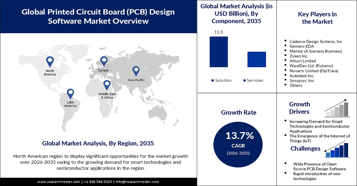
Printed Circuit Board Design Software Market size was over USD 4.12 billion in 2025 and is poised to exceed USD 14.88 billion by 2035, growing at over 13.7% CAGR during the forecast period i.e., between 2026-2035. In the year 2026, the industry size of PCB design software is estimated at USD 4.63 billion.

The PCB design software allows engineers to efficiently design a circuit board which helps to address the abnormalities associated with manufacturing a product. As industries prioritize scalability, faster time-to-market, and global teamwork, cloud adoption is accelerating, making it a key factor in shaping the future of efficient and connected PCB design. In February 2020, Altium launched a cloud-based application A365 Viewer, powered by the Altium 365 cloud platform, offering an advanced way to view and share electronic designs over a browser on any web-enabled desktop, phone, or tablet. These product launches are projected to significantly drive the global market.
The printed circuit board design software market is primarily driven by the increasing demand for high-performance electronic devices, and the shift towards miniaturization and high-density interconnect (HDI) PCBs. In February 2024, IPC and the Printed Circuit Board Association of America (PCBAA) urged Congress to fund the Defense Production Act Purchases Account at the House-passed level of USD 618 million and USD 1.08 billion for the Industrial Base Analysis and Sustainment program. This push drives market growth by boosting investments in U.S.-based PCB production, encouraging the adoption of advanced design software to meet stringent defense requirements.
Key Printed Circuit Board Design Software Market Insights Summary:
Regional Highlights:
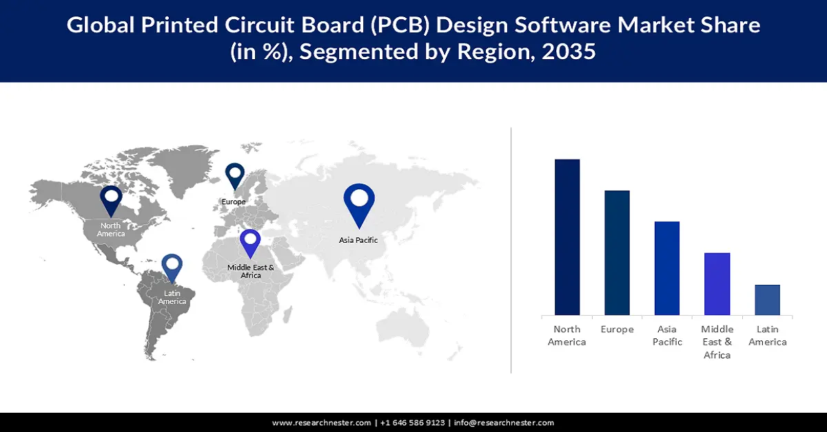
- By 2035, North America is anticipated to secure a 34.7% share of the printed circuit board design software market, propelled by the region’s expanding telecommunications sector and rising semiconductor demand.
- Europe is expected to capture substantial growth through 2035, sustained by increasing adoption of advanced PCB design capabilities such as simulation, thermal stress management, and 3D visualization.
Segment Insights:
- By 2035, the Solution segment in the printed circuit board design software market is projected to command the largest revenue share, fueled by the rising need for integrated, cloud-enabled solutions.
- The On-premises segment is anticipated to secure a leading share by 2035, supported by enterprises’ increasing preference for robust security and advanced customization.
Key Growth Trends:
- Increasing Demand for HDI PCBs
- Next generation solutions with cloud PCB design software
Major Challenges:
- Wide presence of open source PCB design software
- Use of pirated software and a lack of skilled personnel
Key Players: Cadence Design Systems, Inc., Siemens EDA, Mentor (A Siemens Business), Zuken Inc., Altium Limited, WestDev Ltd. (Pulsonix), Novarm Limited (DipTrace), Autodesk Inc., Synopsys, Inc., KiCad.
Global Printed Circuit Board Design Software Market Forecast and Regional Outlook:
Market Size & Growth Projections:
- 2025 Market Size: USD 4.12 billion
- 2026 Market Size: USD 4.63 billion
- Projected Market Size: USD 14.88 billion by 2035
- Growth Forecasts: 13.7%
Key Regional Dynamics:
- Largest Region: North America (34.7% Share by 2035)
- Fastest Growing Region: Europe
- Dominating Countries: United States, China, Japan, Germany, South Korea
- Emerging Countries: India, Vietnam, Malaysia, Mexico, Brazil
Last updated on : 19 November, 2025
Printed Circuit Board Design Software Market - Growth Drivers and Challenges
Growth Drivers
- Increasing Demand for HDI PCBs: High-density interconnects (HDI) PCBs are smaller and lightweight than other PCBs and offer high-speed and reliable signals. Furthermore, they have improved wiring density and lower trace widths. This feature enables fewer layers in the PCB stack and high-speed signal transmission, reducing production expenses. In September 2020, Meiko Electronics Co. Japan purchased multiple ESI® Geode™ systems from MKS Instruments, Inc. to enhance its high-volume HDI PCB manufacturing capabilities in Asia.
- Next-generation solutions with cloud PCB design software: The cloud-based PCB design software makes the work of PCB designers further accurate and reliable. For instance, in April 2022, Frontline Cloud Services, a software solution, launched by KLA Corporation, accelerates design for manufacturing (DFM) analysis and time-to-market (TTM) for complex printed circuit boards (PCBs). Designing exceedingly complicated PCBs is addressed by the new cloud-based SaaS service. As industries demand faster innovation and greater scalability, these tools are becoming essential for enhancing efficiency and reducing costs.
Challenges
- Wide presence of open-source PCB design software: Open-source PCB design software can pose several significant challenges, from unexpected costs and steep learning curves to complex compatibility issues. The majority of open-source vulnerabilities are caused by erroneously designed code that has gaps in it that an attacker might exploit to commit crimes like stealing confidential information or breaking a system.
- Use of pirated software and a lack of skilled personnel: Widespread software piracy leads to revenue losses for vendors and security risks for users. Additionally, the growing complexity of PCB design demands highly skilled professionals. Addressing challenges related to AI-driven automation and high-density PCB layouts requires stronger IP protection measures, industry-driven training programs, and increased adoption of user-friendly AI-assisted design tools.
Printed Circuit Board Design Software Market Size and Forecast:
| Report Attribute | Details |
|---|---|
|
Base Year |
2025 |
|
Forecast Year |
2026-2035 |
|
CAGR |
13.7% |
|
Base Year Market Size (2025) |
USD 4.12 billion |
|
Forecast Year Market Size (2035) |
USD 14.88 billion |
|
Regional Scope |
|
Printed Circuit Board Design Software Market Segmentation:
Component Segment Analysis
The solution segment in the PCB design software market is poised to garner the largest revenue during the forecast period. companies prioritize comprehensive software solutions that offer integrated functionalities like schematic capture, layout design, and manufacturing preparation to streamline the development process. The dominance of the segment is further reinforced by innovations such as Nexar. In April 2021, Altium launched this cloud-based partner platform to enhance collaboration between PCB design software and component manufacturers. This launch highlighted the demand for integrated, cloud-enabled solutions.
Deployment Mode Segment Analysis
The on-premises segment in printed circuit board design software market is expected to witness the highest growth, attributed to its superior security, customization, and control over data. Industries with strict regulations such as aerospace, and defense, prefer on-premises solutions to safeguard intellectual properties and ensure compliance. Additionally, high-performance computing needs and integration with legacy systems drive companies to maintain in-house infrastructure. While cloud adoption is growing, on-premises deployment remains the preferred choice for enterprises requiring robust security and advanced customization.
Our in-depth analysis of the global PCB design software market includes the following segments:
|
Component |
|
|
Type |
|
|
Deployment Mode |
|
|
Organization Size |
|
|
Industry Vertical |
|

Vishnu Nair
Head - Global Business DevelopmentCustomize this report to your requirements — connect with our consultant for personalized insights and options.
Printed Circuit Board Design Software Market - Regional Analysis
North American Market Insights
The North America PCB design software market is projected to hold the largest revenue share of 34.7% by the end of 2035. The region’s telecommunications industry fuels the demand for sophisticated PCB tools capable of handling complex circuit designs. Furthermore, the semiconductor is witnessing a rise in demand in several industries in the U.S. which is also boosting the printed circuit board design software market in the region.
Semiconductor demand share by end use, 2023
|
End use Category |
Demand Share |
|
Communication |
32% |
|
Computer |
25% |
|
Automotive |
17% |
|
Industrial |
14% |
|
Consumer |
11% |
|
Government |
1% |
Source: SIA
Additionally, the region’s focus on AI and machine learning integration in PCB design is transforming automation, optimization, and error detection processes. The presence of major industry players and a highly skilled workforce further solidifies North America’s position as a key market.
The U.S. dominated the North America PCB design software market due to its leadership in defense, aerospace, and consumer electronics. Stringent regulations from bodies such as the FCC and FDA drive the need for compliant and precise PCB layouts, especially in medical and military applications. The country’s demand for advanced driver-assistance systems (ADAS) in automotive electronics is another key driver, boosting PCB tools with high frequency and high-power application demand.
Europe Market Insights
The PCB design software market in Europe is set to garner noteworthy growth in the forthcoming years. The incorporation of services like simulation, thermal stress management, and product lifecycle management are some of the new trends in the market in the region. Furthermore, added features such as 3D design and visualization, integration and import tools, data management, and excellent design capabilities make PCB design software easy to use. For instance, in 2022, Zuken launched its new solution, eCADSTAR, a PCB layout tool with simulation, 3D MCAD integration, and wire harness support. eCADSTAR is offered in a variety of configurations to fulfill different demands resulting in market expansion in Europe.
UK PCB design software market is driven by increased demand for advance electronic devices and a focus on product customization. The expansion is supported by the rising adoption of cloud-based PCB design tools which enhance collaboration and accessibility. Additionally, the shift toward sustainable electronics and miniaturization has encouraged innovation in PBB software that supports flexible and rigid-flex circuits.

Printed Circuit Board Design Software Market Players:
- Cadence Design Systems, Inc.
- Company Overview
- Business Strategy
- Key Product Offerings
- Financial Performance
- Key Performance Indicators
- Risk Analysis
- Recent Development
- Regional Presence
- SWOT Analysis
- Siemens EDA
- Mentor (A Siemens Business)
- Zuken Inc.
- Altium Limited
- WestDev Ltd. (Pulsonix)
- Novarm Limited (DipTrace)
- Autodesk Inc.
- Synopsys, Inc.
- KiCad
- Other key players
Key companies in the printed circuit board design market are focusing on AI-driven automation, cloud-based collaboration, and seamless integration with manufacturing processes. Industry trends include the rise of 3D PCB design, real-time simulation tools, and open-source platforms to enhance accessibility. Companies are also leveraging mergers and acquisitions to expand capabilities and cater to growing needs. Some of the key companies are:
Recent Developments
- In October 2024, CELUS announced its collaboration with Siemens Digital Industries Software to enhance accessibility and efficiency in PCB design for small to medium-sized businesses (SMBs) and independent engineers.
- In February 2023, Pulsonix version 12.0 was introduced by Pulsonix, which encompasses new characteristics such as speed augmentation with highly requested usability improvements. The new version is faster as compared to the older version because of the additional multi-threading capabilities as well as the improved 64-bit implementation to fasten the time-consuming features.
- In December 2022, Zuken Ltd. declared improving support for power module design, created with the Compound Semiconductor Applications (CSA) Catapult in South Wales, a non-profit supported by the UK government. CSA Catapult was established to help the UK in becoming a global leader in compound semiconductors.
- Report ID: 92
- Published Date: Nov 19, 2025
- Report Format: PDF, PPT
- Explore a preview of key market trends and insights
- Review sample data tables and segment breakdowns
- Experience the quality of our visual data representations
- Evaluate our report structure and research methodology
- Get a glimpse of competitive landscape analysis
- Understand how regional forecasts are presented
- Assess the depth of company profiling and benchmarking
- Preview how actionable insights can support your strategy
Explore real data and analysis
Frequently Asked Questions (FAQ)
Printed Circuit Board Design Software Market Report Scope
Free Sample includes current and historical market size, growth trends, regional charts & tables, company profiles, segment-wise forecasts, and more.
Connect with our Expert
Copyright @ 2026 Research Nester. All Rights Reserved.


