Copper Sputtering Target Market Outlook:
Copper Sputtering Target Market size was valued at USD 1.44 billion in 2025 and is likely to cross USD 3 billion by 2035, registering more than 7.6% CAGR during the forecast period i.e., between 2026-2035. In the year 2026, the industry size of copper sputtering target is assessed at USD 1.54 billion.
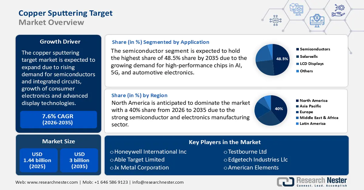
The rising demand for semiconductors and integrated circuits is one of the primary reasons for the growth of the copper sputtering target market. Copper is widely used in integrated circuits and semiconductors, replacing aluminum due to its superior electrical conductivity, low power consumption, and increased processing speeds. With the rapid development of technologies such as AI chips, 5G networks, and cloud computing, the semiconductor industry is experiencing significant expansion. This drives the need for high-quality copper films used in integrated circuits.
The global push towards renewable energy sources has resulted in rapid growth in the solar PV sector. Copper sputtering targets are used in the manufacturing of thin film solar cells, which are pivotal for converting sunlight into electricity efficiently. Moreover, the rising focus on renewable energy and government incentives for solar power projects drive the production of solar panels, thereby bolstering the demand for high-quality copper sputtering targets.
Key Copper Sputtering Target Market Insights Summary:
Regional Highlights:
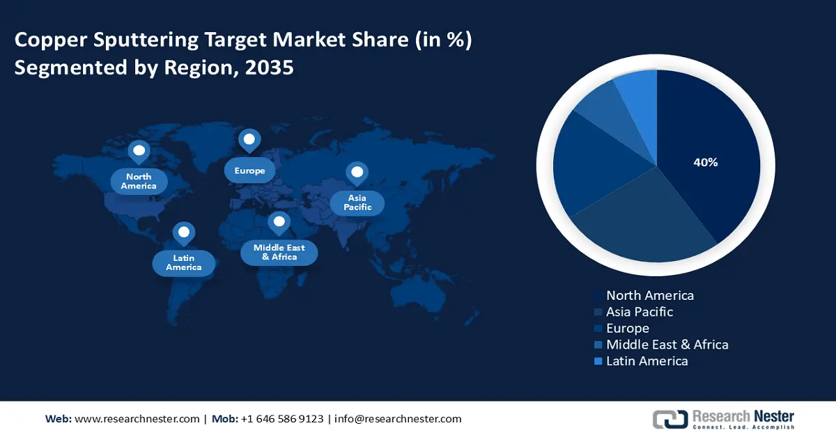
- North America dominates the Copper Sputtering Target Market with a 40% share, driven by semiconductor, electronics manufacturing, and investments under the CHIPS Act, supporting growth through 2035.
- Asia Pacific's Copper Sputtering Target Market is anticipated to experience rapid growth from 2026–2035, fueled by leadership in semiconductor fabrication and EV adoption.
Segment Insights:
- The Semiconductors segment is projected to hold a 48.5% share by 2035, driven by surging demand for high-performance chips in AI, 5G, and automotive electronics.
Key Growth Trends:
- Growth of consumer electronics and advanced display technologies
- Deployment of 5G and AI technology
Major Challenges:
- High purity copper supply constraints and price volatility
- Performance and waste management issues in thin film deposition
- Key Players: Honeywell International Inc., Able Target Limited, Advanced Engineering Materials Limited, American Elements, Edgetech Industries Llc, Jx Metals Corporation.
Global Copper Sputtering Target Market Forecast and Regional Outlook:
Market Size & Growth Projections:
- 2025 Market Size: USD 1.44 billion
- 2026 Market Size: USD 1.54 billion
- Projected Market Size: USD 3 billion by 2035
- Growth Forecasts: 7.6% CAGR (2026-2035)
Key Regional Dynamics:
- Largest Region: North America (40% Share by 2035)
- Fastest Growing Region: Asia Pacific
- Dominating Countries: United States, China, Japan, Germany, South Korea
- Emerging Countries: China, Japan, South Korea, Taiwan, India
Last updated on : 12 August, 2025
Copper Sputtering Target Market Growth Drivers and Challenges:
Growth Drivers
- Growth of consumer electronics and advanced display technologies: The rising demand for smartphones, laptops, tablets, and gaming consoles increases the need for copper-based thin films in printed circuit boards (PCBs). The rising trend in wearable technology, foldable and flexible electronics, and AR/VR create new opportunities for high-quality, precise copper coatings. For instance, a notable recent example illustrating the expansion of consumer electronics and advanced display technologies is Samsung’s newly developed display concept in March 2025. The company unveiled a stretchable screen, a foldable gaming console, and a TV that folds to fit into a briefcase.
- Deployment of 5G and AI technology: The widespread adoption of 5G networks and the development of AI applications necessitate advanced electronic infrastructure. This infrastructure relies heavily on high-performance electronic components driving the demand for copper sputtering targets. According to a 2023 report published by IEEE International Roadmap for Devices and Systems, using AI and IoT has brought innovation to the semiconductor industry. The integration of IoT can turn ordinary objects into smart devices and enhance economic opportunities. Furthermore, the integration of AI and IoT is expected to generate revenue of USD 3.9 trillion to USD 11.1 trillion by 2025.
Challenges
- High purity copper supply constraints and price volatility: The production of high purity i.e., 99.9% or 5N copper sputtering targets requires refined raw materials, which are limited and expensive. Copper prices are highly volatile due to fluctuations in mining output, geopolitical factors, and global demand from industries like EVs and construction. Additionally, supply chain disruptions due to geopolitical tensions, trade restrictions, and raw material shortages affect manufacturing and hamper stable pricing.
- Performance and waste management issues in thin film deposition: Copper sputtering targets tend to wear unevenly, leading to material waste and inconsistent film thickness, impacting semiconductor and electronics manufacturing. Recycling using targets is challenging due to contamination and the complexity of recovering high-purity copper. Thus, improving target utilization efficiency and developing new recycling technologies are crucial to reducing costs and environmental impact.
Copper Sputtering Target Market Size and Forecast:
| Report Attribute | Details |
|---|---|
|
Base Year |
2025 |
|
Forecast Period |
2026-2035 |
|
CAGR |
7.6% |
|
Base Year Market Size (2025) |
USD 1.44 billion |
|
Forecast Year Market Size (2035) |
USD 3 billion |
|
Regional Scope |
|
Copper Sputtering Target Market Segmentation:
Application (Semiconductors, Solar Cells, LCD Displays)
Semiconductor segment is projected to account for copper sputtering target market share of more than 48.5% by the end of 2035, due to the growing demand for high-performance chips in AI, 5G, and automotive electronics. The demand for semiconductors is increasing due to their wide applications, and are the most in-demand product. The OEC Report reveals that semiconductor devices were the world's 21st most traded product in 2023, with a total trade value of USD 155 billion. As semiconductor manufacturers transition to smaller nodes, i.e., 3nm and below, high-purity copper is becoming essential for interconnects and advanced packaging. The rise of chiplet designs and heterogeneous integration is further increasing the need for precise thin film deposition using copper sputtering.
The trend toward miniaturization is transforming electronic devices into smaller, portable, and more powerful, thus increasing the demand for semiconductors. Top manufacturing firms are competing to develop miniature semiconductor chips. For instance, in March 2024, Marvell Technology Inc. collaborated with TSMC to become the first technology platform to develop 2nm semiconductors, particularly for accelerated infrastructure. Leading semiconductor hubs such as Japan, Taiwan, and the U.S. are ramping up domestic chip production, driving steady demand for copper targets. With ongoing advancements in logic chips, memory devices, and high-speed computing, the market for copper sputtering targets is set for sustained growth.
End Use (Electronics, Automotive, Aerospace and Defense, Medical Device, Renewable Energy)
In copper sputtering target market, electronics segment is expected to hold revenue share of over 35% by the end of 2035, owing to its applications in PCBs, semiconductors, and display technologies. The rise of wearable tech, AR/VR devices, and IoT gadgets is increasing the demand for precise copper coatings for improved performance. As 5G, AI, and high-performance computing expand, the need for more advanced copper sputtering targets arises leaving scope for the market to grow.
Our in-depth analysis of the global copper sputtering target market includes the following segments:
|
Application |
|
|
End use |
|
|
Type |
|
|
Purity Level |
|

Vishnu Nair
Head - Global Business DevelopmentCustomize this report to your requirements — connect with our consultant for personalized insights and options.
Copper Sputtering Target Market Regional Analysis:
North America Market Analysis
North America copper sputtering target market is poised to capture revenue share of around 40% by the end of 2035, due to the strong semiconductor and electronics manufacturing sector. With the rise of 5G, AI, and data centers, there is a growing demand for high-purity copper thin films in chips and advanced display technologies. Many investments in domestic and semiconductor fabs driven by the CHIPS Act are further boosting the need for copper-based interconnects. Additionally, the increasing adoption of smartphones, AR/VR devices, and electric vehicles is propelling demand for copper sputtering in next-generation electronics.
The U.S. copper sputtering target market is thriving due to the dominant semiconductor manufacturing, consumer electronics, and high-performance computing. Government initiatives such as the CHIPS and Science Act are accelerating domestic semiconductor production, increasing demand for high-purity copper sputtering targets in integrated circuits, memory chips, and advanced microprocessors. According to the SIA, the U.S. retains nearly 46% of the revenue share for cumulative semiconductor sales. Thus, with rising investments, and R&D, the U.S. is reinforcing its leadership in advanced electronics and copper sputtering applications.
In Canada, the copper sputtering market is expanding primarily due to EV battery advancements, green energy technologies, and next-generation consumer electronics. The country’s push for electric vehicle production and battery innovation has led to increased demand for copper-based thin films in power electronics and solid-state batteries. Additionally, Canada is investing heavily in nanotechnology and advanced display manufacturing creating new opportunities for copper sputtering in OLED screens, quantum dot displays, and energy-efficient smart devices. For instance, in September 2023, Volta Energy Solutions, a pioneer in manufacturing electro-deposited copper foil for batteries, entered the Canada copper sputtering target market by establishing a manufacturing plant in Quebec, Canada. This facility aims to address the growing demand for high-quality copper foil in North America’s electric vehicle battery supply chain. In Canada, the focus on EV battery production and clean energy technologies is increasing the need for high purity copper thin films. This development highlights the country’s commitment to advancing EV battery technology and strengthening its position in the copper sputtering target market.
Asia Pacific Market Analysis
Asia Pacific is anticipated to garner a notable share from 2026 to 2035 driven by the region’s leadership in semiconductor fabrication, high-end electronics, and display panel manufacturing. Countries such as China, Japan, and South Korea are heavily investing in advanced chip technologies and OLED production, driving demand for high-purity copper targets. The rapid adoption of electric vehicles and energy-efficient devices is further boosting copper sputtering applications. With continuous technological innovation and strong industrial infrastructure, Asia Pacific remains the fastest-growing market for copper sputtering targets globally.
China’s copper sputtering target market is expanding as the country accelerates its dominance in semiconductor and high-tech manufacturing. With heavy investments in domestic chip production, AI-driven computing, and 5G technology, the demand for high-purity copper thin films is rising. Additionally, China’s push for renewable energy and EV battery advancements is increasing the use of copper coatings in power electronics. With strong government backing and continuous R&D in next-generation electronics, China is likely to be a key player in the global market.
The copper sputtering target market in South Korea is expanding due to its leadership in semiconductor memory, OLED displays, and high-performance electronics. The country leads in next-generation semiconductor technology, where high-purity copper thin films are needed for high-speed processing and miniaturized circuits. With the rise of foldable displays, 6G research, and AI-driven devices, the demand for copper sputtering targets in display and sensor technologies is increasing. Backed by government initiatives and private sector R&D, South Korea is enhancing its role as a global hub for high-tech materials and chip manufacturing.
Key Copper Sputtering Target Market Players:
- Honeywell International Inc.
- Company Overview
- Business Strategy
- Key Product Offerings
- Financial Performance
- Key Performance Indicators
- Risk Analysis
- Recent Development
- Regional Presence
- SWOT Analysis
- Able Target Limited
- Advanced Engineering Materials Limited
- American Elements
- Edgetech Industries Llc
- Jx Metals Corporation
- Konfoong Materials International Co., Ltd
- Kurt J. Lesker Company
- Nanoshel Llc.
- Otto Chemie Pvt. Ltd.
- Praxair Technology, Inc
- Safina Materials, Inc
- Testbourne Ltd
- Tosoh Smd, Inc
- Vacuum Engineering & Materials
The top companies dominating the copper sputtering target market specialize in producing high-purity copper targets for semiconductors, display panels, and advanced electronics. With continuous R&D investments and technological innovations, they play a crucial role in meeting the growing demand for high-performance thin films globally. Here are some leading players in the copper sputtering target market:
Recent Developments
- In October 2024, DIC Corporation created a new polyphenylene sulfide (PPS) film in partnership with the Japanese company Unitika Ltd. This film reduces signal loss at high frequencies, making it ideal for millimeter wave printed circuit boards used in next generation communication devices and radar systems.
- In January 2024, SC successfully developed new equipment for coating copper foil using a roll-to-roll magnetron sputtering process. This achievement expanded SC’s opportunities in the vacuum equipment market for composite materials and current collectors. It also marks a significant breakthrough in producing specialized vacuum equipment for lithium-ion battery manufacturing.
- Report ID: 7359
- Published Date: Aug 12, 2025
- Report Format: PDF, PPT
- Explore a preview of key market trends and insights
- Review sample data tables and segment breakdowns
- Experience the quality of our visual data representations
- Evaluate our report structure and research methodology
- Get a glimpse of competitive landscape analysis
- Understand how regional forecasts are presented
- Assess the depth of company profiling and benchmarking
- Preview how actionable insights can support your strategy
Explore real data and analysis
Frequently Asked Questions (FAQ)
Copper Sputtering Target Market Report Scope
Free Sample includes current and historical market size, growth trends, regional charts & tables, company profiles, segment-wise forecasts, and more.
Connect with our Expert


Copyright @ 2026 Research Nester. All Rights Reserved.
